PL
Detection principle
· Photoluminescence (PL for short), the defects of solar cells often limit their photoelectric conversion efficiency and service life
· Photoluminescence can quickly detect silicon wafers through the change of minority carrier lifetime. The principle is to use the principle of photoluminescence to obtain fluorescent photos of crystalline silicon, and it has high resolution to detect the rough surface and internal damage of silicon wafers.
· Compared with the EL test, which needs to touch the sample, the PL test does not touch the sample, so it can monitor the production process of the production cell
| Project | Specification |
| Equipment size | Length 450mm Width 450mm Height 770mm |
| Applicable maximum size | 175*175mm |
| Applicable Wafer Type | Single crystal, polycrystalline |
Maximum capacity | >3600PCS/hour |
| Pixel Accuracy | <0.34mm (0.5K line scan camera) |
| Detection accuracy | <0.34mm |
UPTime | >98% |
| Project | Specification |
Black heart, black edge, black | Single crystal, polycrystalline |
| Crack | Single crystal, polycrystalline |
| Scratches | Single crystal, polycrystalline |
Pollute | Single crystal, polycrystalline |
| Broken grid | Single crystal, polycrystalline |
Uneven sintering | Single crystal, polycrystalline |
| Dislocation | Polycrystalline |
| Damaged | Single crystal, polycrystalline |
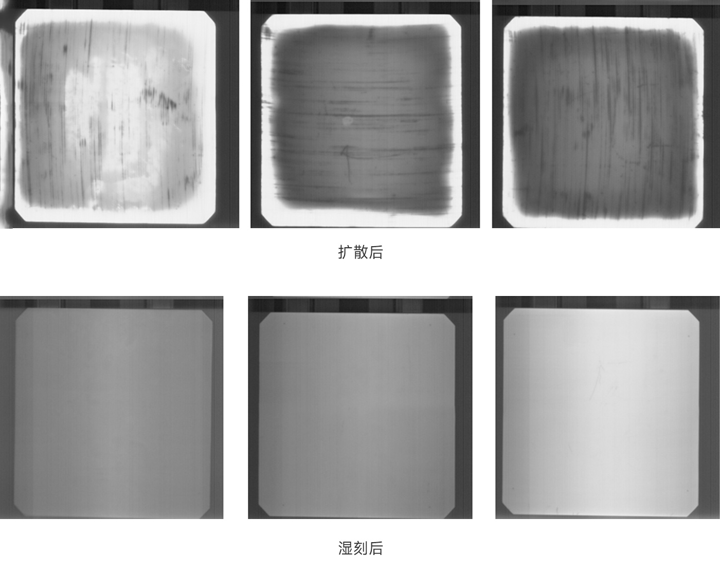
Imaging effect


 明升国际_明升国际科技有限公司
welcometo欢迎光临888集团(中国)有限公司
凯发k8官网(中国)登录vip入口
k8凯发(中国)天生赢家·一触即发
918博天堂(中国区)官方网站